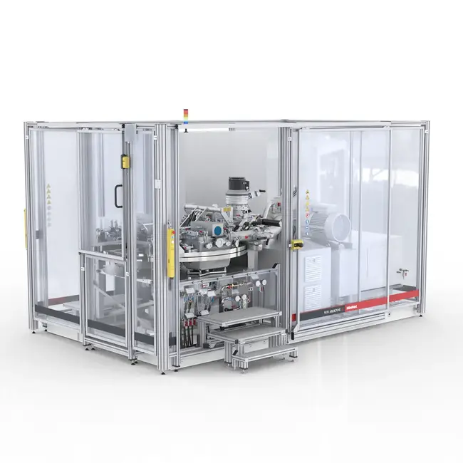
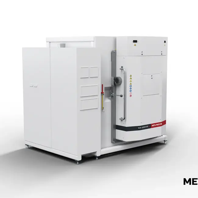
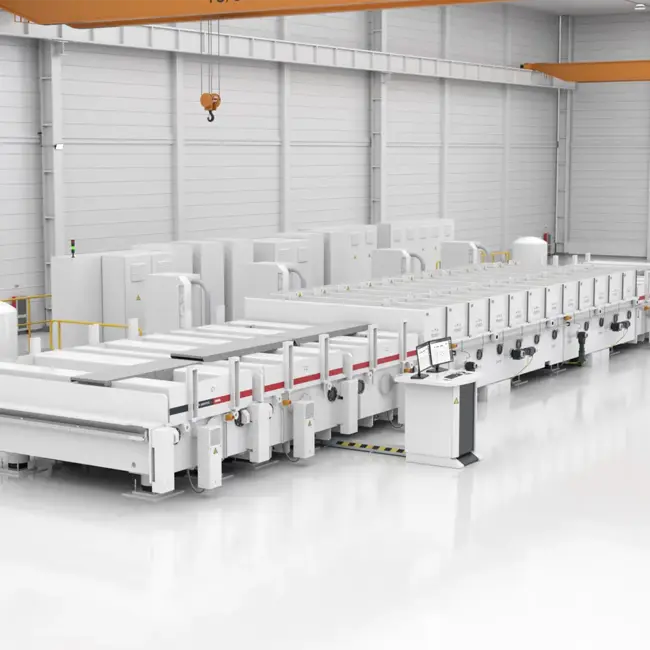
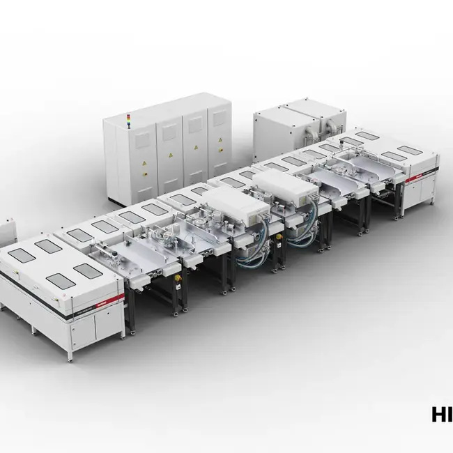
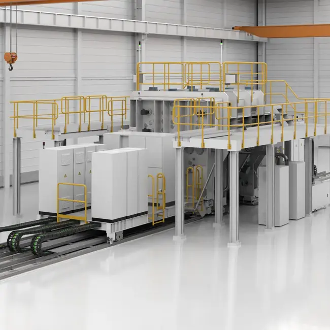
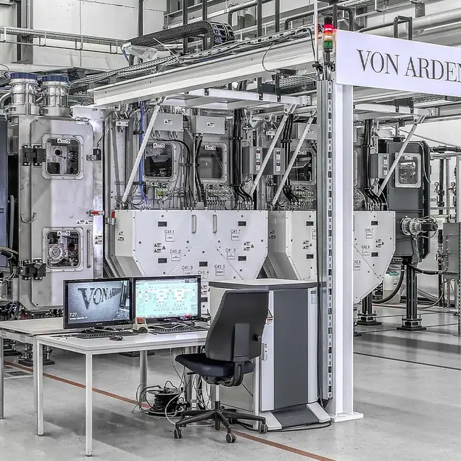
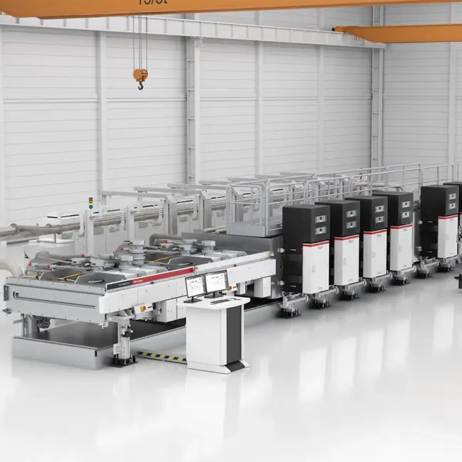
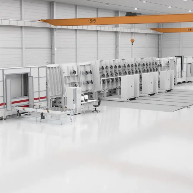
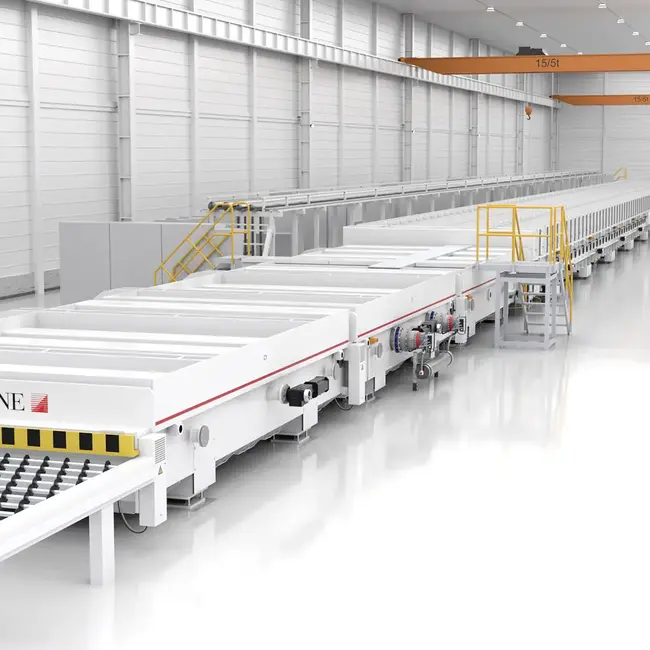
Equipment
Equipment
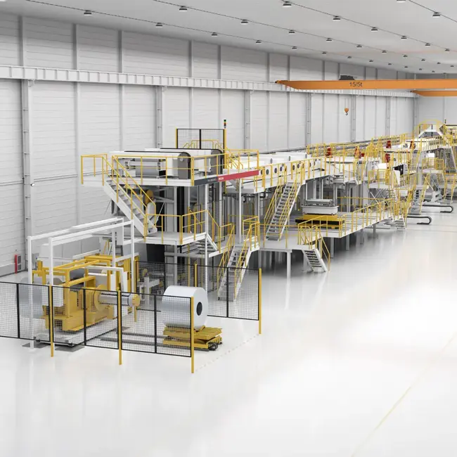
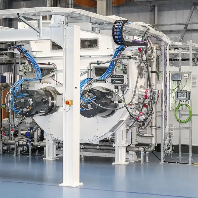
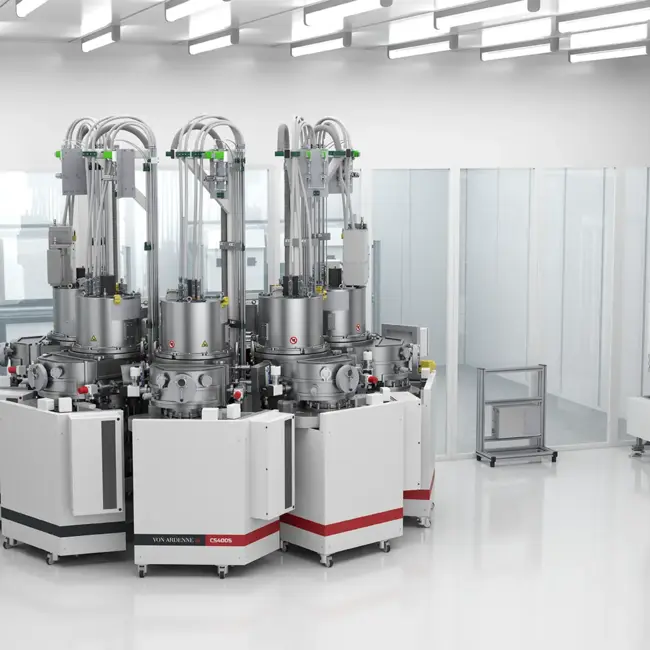
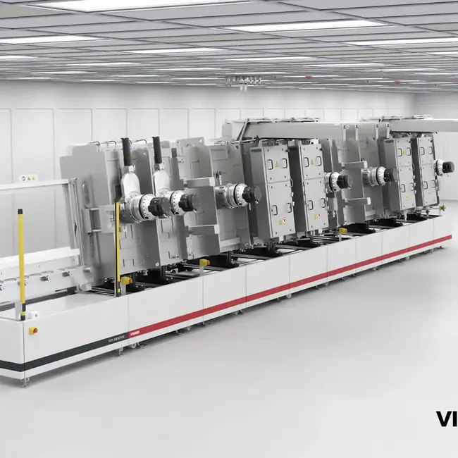
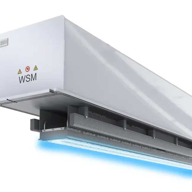
One of our most important core technologies is magnetron sputtering. In this process, the coating material is removed from a solid target and transferred to the substrate.
This is done in a magnetic field-enhanced gas discharge in a vacuum. This discharge creates a plasma, a mix of electrons and positive gas ions. The positively charged ions are accelerated by an electric field onto the surface of the target, which is connected as a cathode. This knocks individual atoms out of the target surface.
These atoms condense on a substrate, for example glass, and form the functional layer. The substrate is either continuously moved past the magnetron sputter source (dynamic coating) or exposed to the vapor flow for a defined time (static coating). In dynamic coating, the thickness of the layer is determined by the rate of material removal from the target and the speed at which the substrate passes. In static coating, the dwell time determines the thickness.
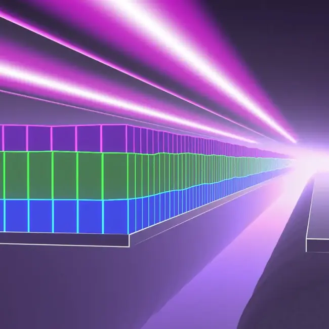
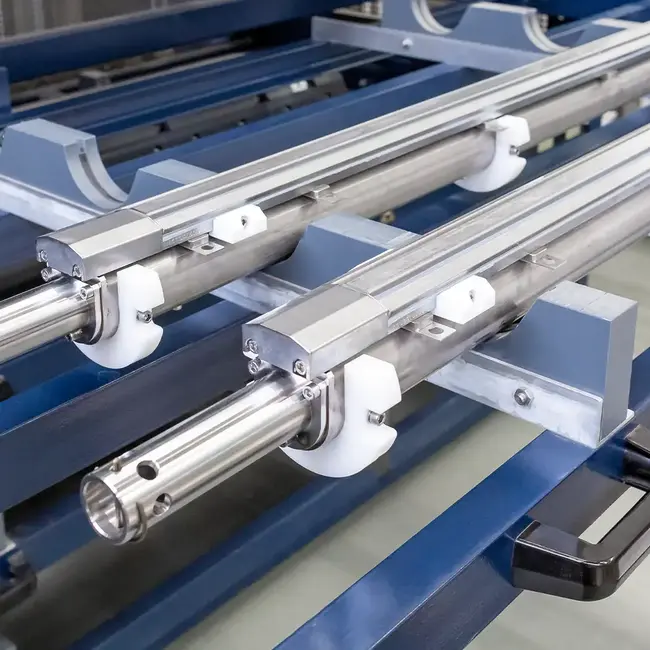
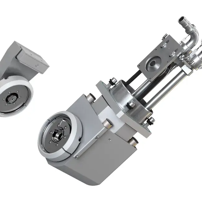
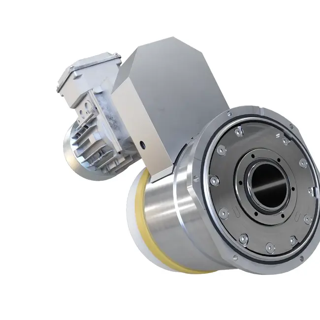
Magnetron sputtering can be used for a variety of metallic and ceramic coating materials. Depending on the process, complex coatings with a thickness of up to several hundred nanometers can be deposited very efficiently and with high uniformity on large areas. Depending on the application, tubular or planar targets are used, the length of which can be scaled with the width of the substrates to be coated.
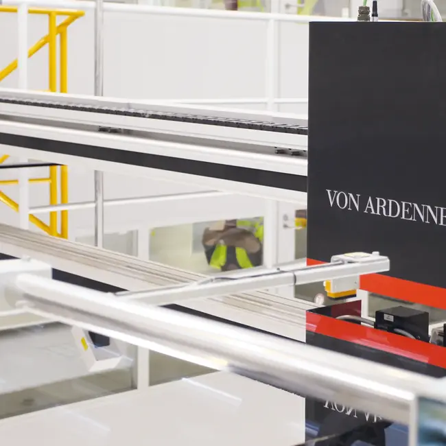
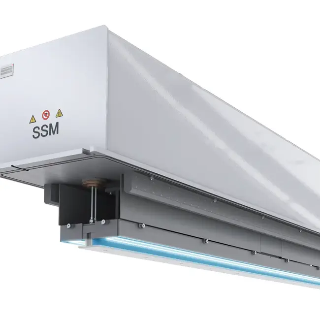
Magnetrons are key components at VON ARDENNE. We develop and manufacture the magnetrons in-house. This allows us to incorporate the extensive knowledge we have gained from hundreds of delivered systems and components.
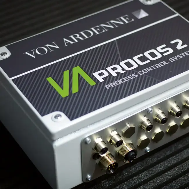
Would you like to learn more? Then click on the content below or contact us directly.
for a wide range of sputtering applications
of high homogeneity on small and large areas
from in-house development & manufacturing
Boston, MA, USA
Phoenix, AZ, USA
Phoenix Convention Center
Booth 6180