Wafer-Level Optics
Coating Equipment for Precision Optical Components

Optical filter layers deposited directly on glass or semiconductor wafers enable optical products that have a very small size and a competitive price-performance ratio. Therefore, they have found their way into various markets such as consumer electronics or the automotive industry. Due to the increasing demand for high volume production, wafer-level optics are becoming the focus of the industry.

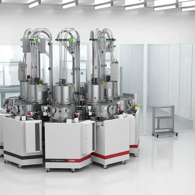
With the OPTA X, we offer you a coating system that has been specially developed to meet the requirements in the fields of photonics and wafer level optics.

For multilayer coating of wafer-based microlens arrays, semiconductor sensors or filter-on-chip CMOS, the OPTA X provides you with fully automated, SEMI-compatible wafer handling for integration in semiconductor fabs. In addition to wafers with a diameter of 200 millimeters, the OPTA X is also suitable for wafer sizes up to 300 millimeters.

Would you like to learn more? Then click on the individual products below or contact us directly.

Optical filter layers directly on glass and semiconductor wafers

 e.g. for silicon devices

Optical monitoring of transmission or reflection

directly on the wafer

SEMI-compatible wafer handling

for integration in semiconductor fabs

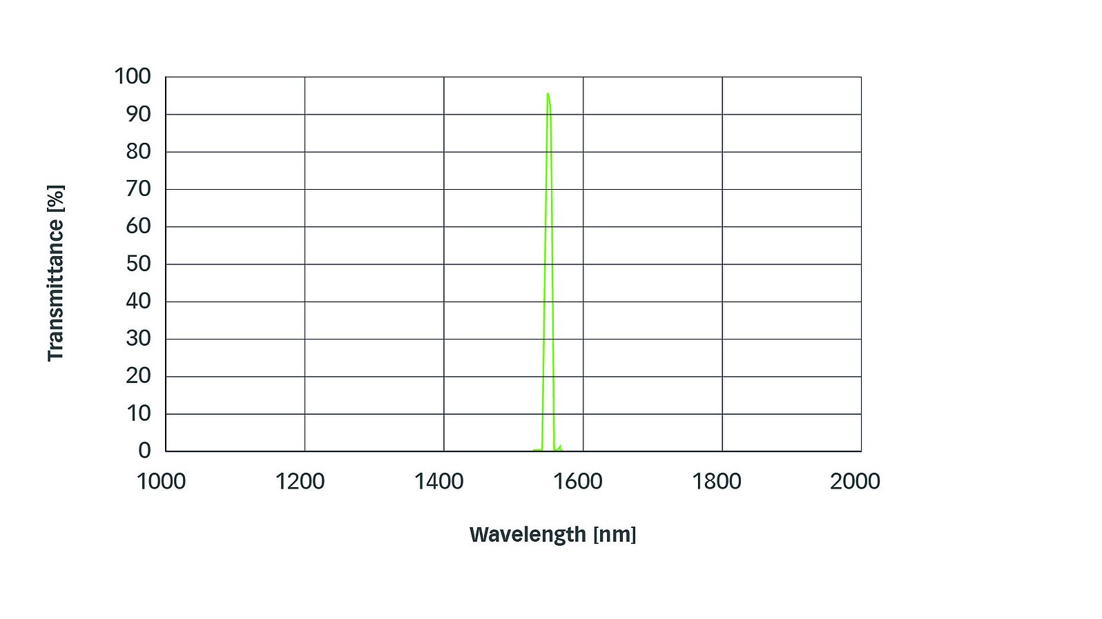
Narrow-Band Filter
Coating Example

Support
Media
Customer Portal "myVA" Now Available

It's here: the myVA Customer Portal. VON ARDENNE has developed it with the aim of simplifying interactions, providing valuable insights and increasing…

CONTACT
24.06.2025 - 27.06.2025
Laser World of Photonics 2025

München, Deutschland

Messegelände München


Michael Schneider

Industry Manager OpticsVON ARDENNE GmbH

Search