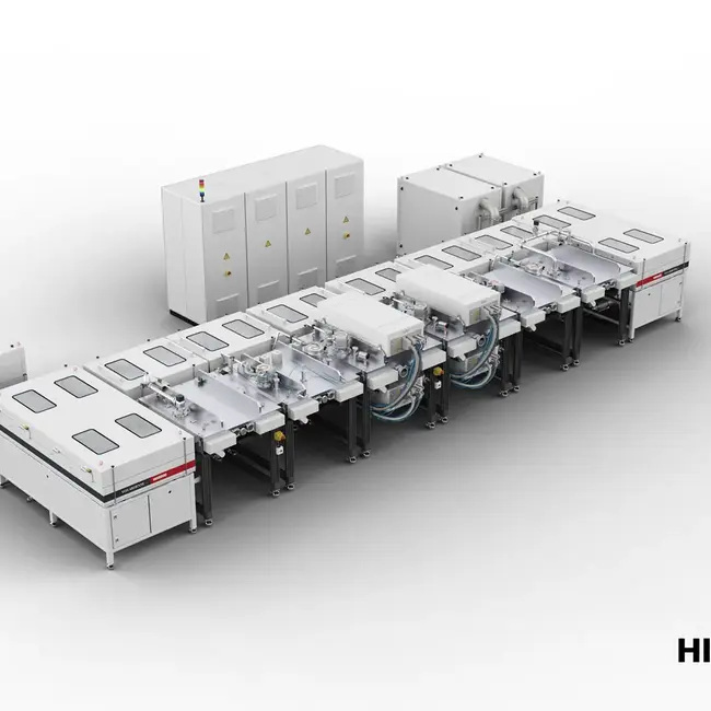
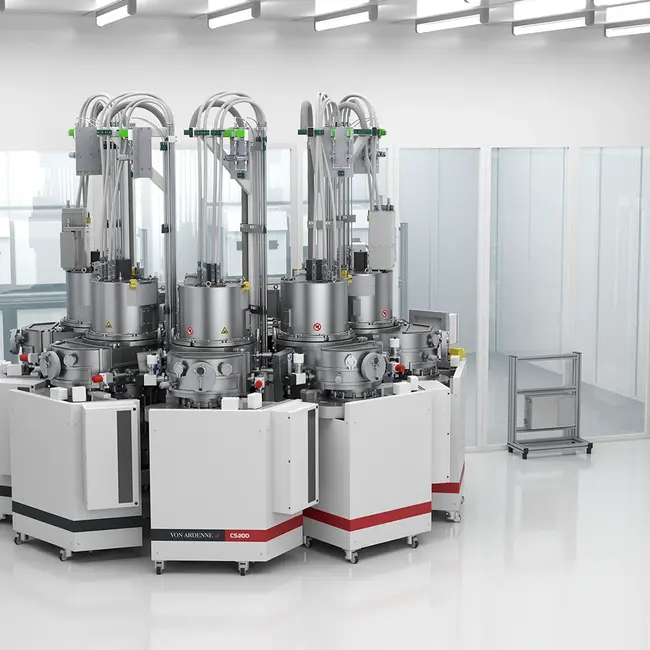
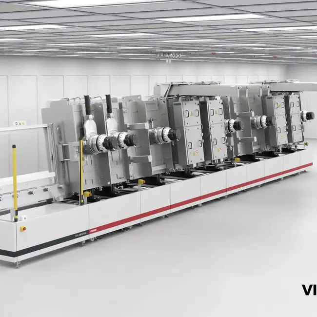
Advanced Packaging
Pioneering Vacuum Deposition Equipment for Wafer or Panel-Level Substrates

There are many approaches to semiconductor advanced packaging, the art of efficiently and compactly connecting multiple chips to maximize system performance. 

Increasingly complex electrical systems are created by advanced packaging approaches. As a result, the requirements for the conductive and insulating layers are becoming more complex. At the same time, the substrates and the utilization of the available area must be optimized to manufacture these devices cost-effectively.

Materials, and the processes used to deposit them, are increasingly complex, demanding highly engineered platforms that can solve the most complex metallization challenges for high-aspect-ratio structures. And this is where we excel: materials and equipment innovation, on wafer or panel substrates, with sub-nanometer precision. 

Would you like to learn more? Explore the content below or contact us.

Highly productive system platform

based on extensive process know-how

Easy adaptation to new processes & requirements

due to flexibly configurable equipment

Cost-efficient equipment

due to fully automated concept

CLEANROOM
VA CLEANROOM
Cleanroom-Compatible Sampling & Assembly Facility

for precision optics, photonics & semiconductor applications

  • Manufacturing of vacuum coating systems
  • Sampling & pilot deposition services
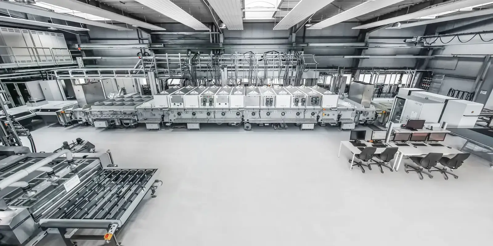
  • 600 m² semiconductor cleanroom including AMC capability
Support
Media
VON ARDENNE Unveils New Cleanroom at Headquarters

State-of-the-art facility for sampling, assembly and commissioning

VON ARDENNE Launches New OPTA X300 Deposition Tool and Opens New Cleanrooms in Dresden, Germany

Company showcases its advanced engineering capabilities and new deposition solutions at SEMICON West

CONTACT
07.10.2025 - 09.10.2025
Semicon West 2025

Phoenix, AZ, USA

Phoenix Convention Center

Booth 6180

Sven Frauenstein

Vice President Semiconductor

Search