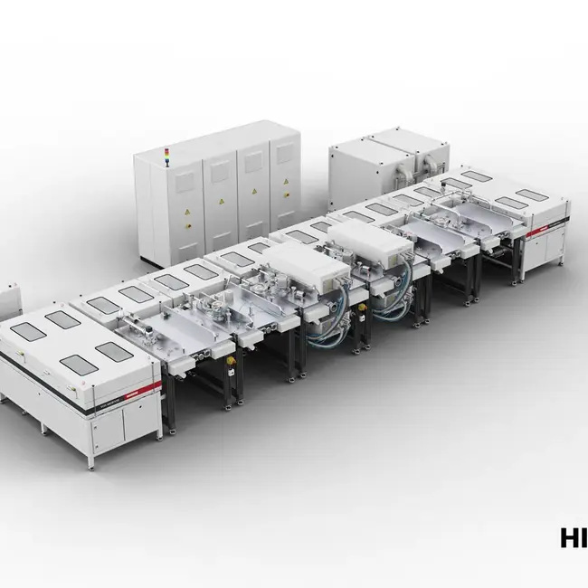
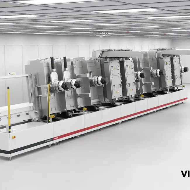
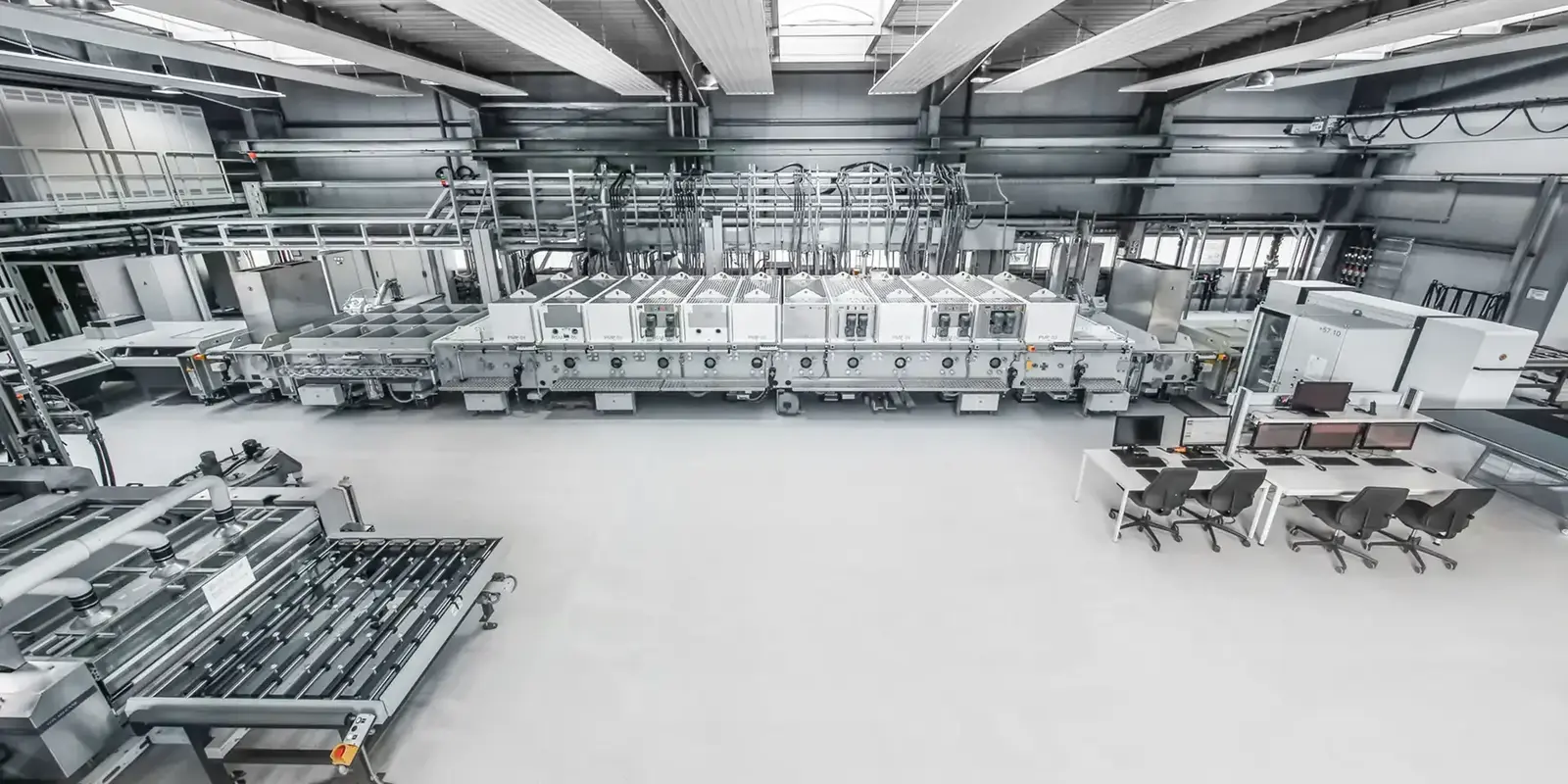
CLEANROOM
VA CLEANROOM
Cleanroom-Compatible Sampling & Assembly Facility
for precision optics, photonics & semiconductor applications

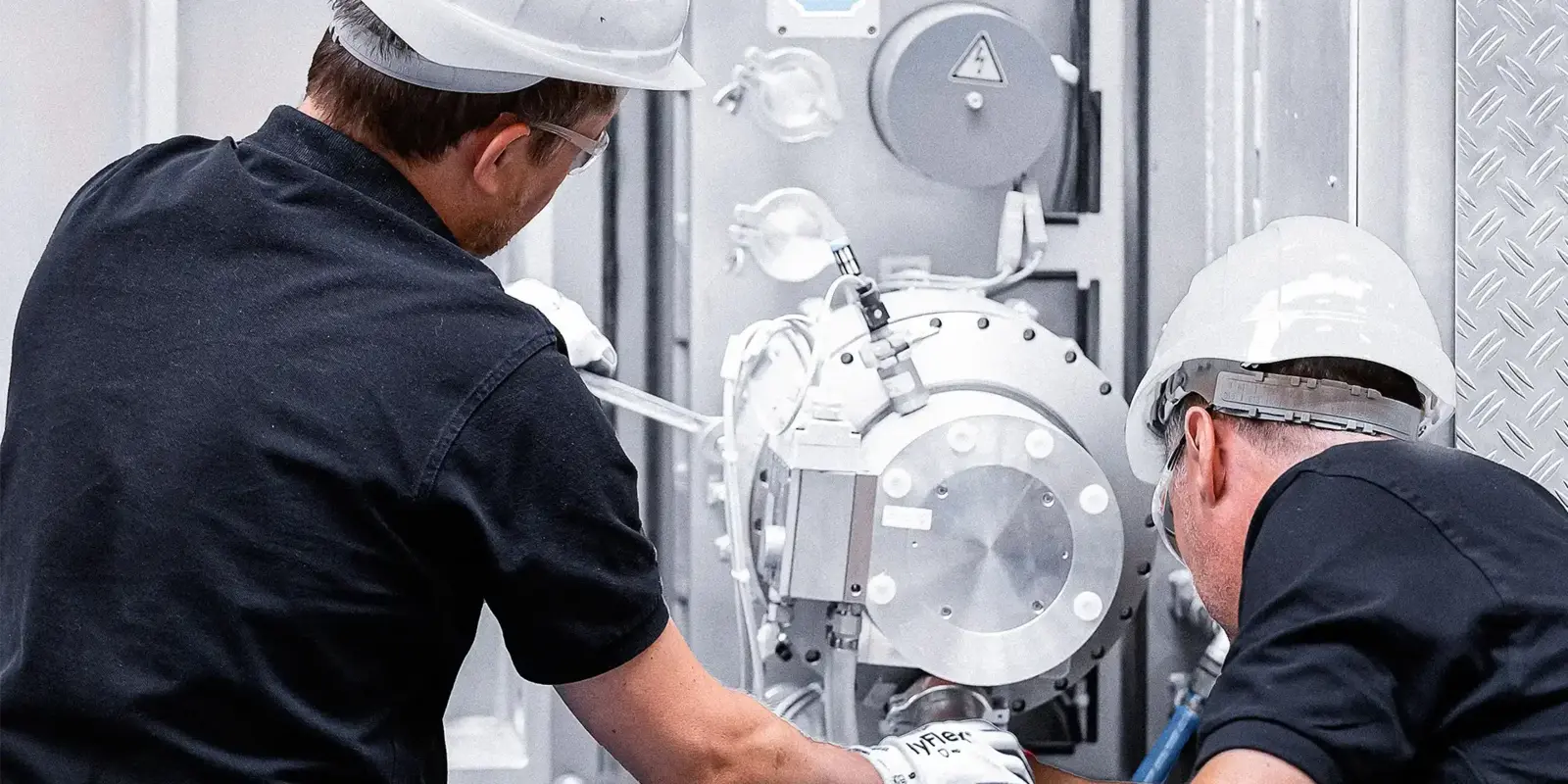
- Manufacturing of vacuum coating systems
- Sampling & pilot deposition services
- 600 m² semiconductor cleanroom including AMC capability
Support
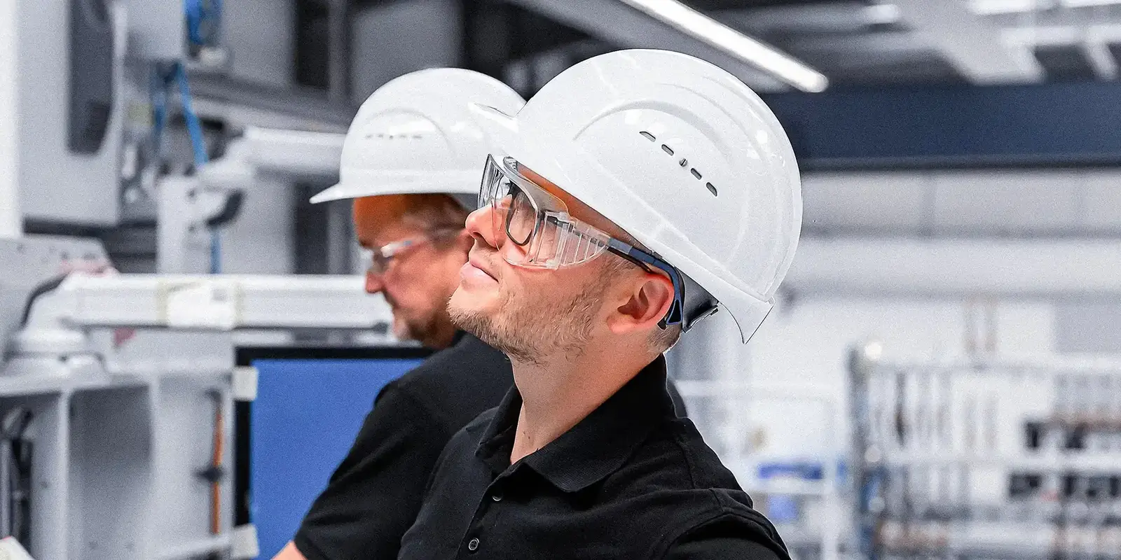
Engineering
Simulation . Sampling . Layout
Technology & Application Center
Sampling . Development . Scaling
Service
Customer Portal . Spare Parts . Trainings
CONTACT
07.10.2025 - 09.10.2025
Semicon West 2025
Phoenix, AZ, USA
Phoenix Convention Center
Booth 6180