At that time, the production of resistors, transistors and rectifiers gained traction. Furthermore, the established evaporation methods were reaching their limits. There was a demand for new, efficient technologies for the increasingly precise coatings of parts that kept getting smaller. This is when the era of the planar magnetron began. This was not least because with magnetron sputtering it was possible to deposit considerably more material than with evaporation. Consequently, the technology could be used in a wider range of applications.
Magnetrons in many shapes
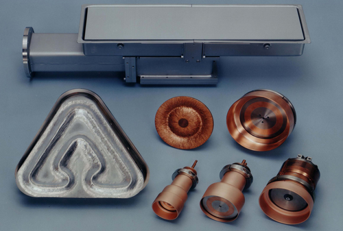
This new technology could be adapted to the respective requirements by different geometries of the targets and arrangements of the magnetic field. As a result, magnetrons were built in a multitude of shapes and forms (see picture) – ranging from diameters of a few centimeters to lengths of several meters. The magnetrons were powered by one to 100 kilowatts.
Triangular magnetrons were used when the substrates were arranged on a rotary disc. Long rectangular magnetrons were the right choice for the coating of large areas on substrates such as glass panes or polymer films. In 1983, the Manfred von Ardenne Research Institute (IvA) equipped the first inline glass coating systems in the GDR with 1.8 meters long sputtering sources, which had a maximum power of 25 kilowatts.
First sputter system for microelectronics
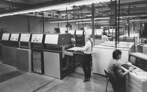
Even earlier, in the late 1970ies, the IvA had developed the first horizontal sputter system HZM-4P, together with the Center for Research and Technology in Microelectronics (ZFTM). Soon after that, a modular inline version followed. More than 100 of these machines were used in the electronics production in the GDR. What is remarkable is that in West Germany comparable systems were only built several years later.
The sputter systems were initially used for high-rate sputtering of metals and alloys in DC mode. But the demand for non-conductive ceramic layers was increasing and the sputtering sources were suited to meet this demand.
The onset of reactive sputtering
Reactive magnetron sputtering is considered a further step in the development of the technology. This method was initially restricted to conductive targets as a DC-powered process. One of its challenges was to control the reactive plasma in the plasma to achieve optimal coating results at high rates. And again, it was a group of IvA employees that developed a solution for process control with the plasma emission monitor (PEM). The ability to control the various parameters during a sputtering process became a central field of development regarding the optimization of magnetron sputtering in the decades that followed.
Up to that point, the above-mentioned methods had established themselves as the standard, but soon, their efficiency and relatively low target utilization proved to be limiting factors. Even though the potential solutions were known, putting them into practice was still difficult. One of these new approaches was the use of moveable magnets or targets until rotatable magnetrons - tubular sputter sources that rotated – became the standard.
Up to that point, the above-mentioned methods had established themselves as the standard, but soon, their efficiency and relatively low target utilization proved to be limiting factors. Even though the potential solutions were known, putting them into practice was still difficult. One of these new approaches was the use of moveable magnets or targets until rotatable magnetrons - tubular sputter sources that rotated – became the standard.
In the next article, we will explore the challenges in the development of rotatable magnetrons and how VON ARDENNE managed to make it happen.
---
Don't miss the first article of this series: Magnetron Sputtering: How It Began

